Printed Circuit Board (PC Manufacturing Process Overview
Overview of PCB manufacturing process
PCBs are initially manufactured using two types of software. Computer-aided design (CAD) software is used to design the electronic schematic of the circuit to be produced. After designing the schematic, engineers use computer-aided manufacturing (CAM) software to create a PCB prototype.
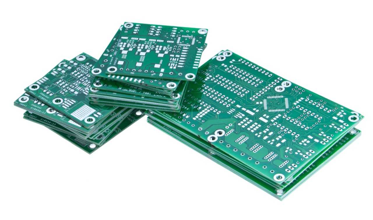
After the electronic PCB assembly (https://www.viasionpcb.com/) is complete, the first step in the manufacturing process is the selection of the PCB material. There are many different types of PCB materials available, but depending on the application and customer requirements, the most popular materials include: Alumina, Arlon, Bakelite, CEM1, CEM5, Ceramic, FR1, FR4, High Temp FR4, GeTek, Nelco, Polyimide and Rogers. Design requirements determine the dimensions (i.e., length, width, and thickness) of the PCB.
After selecting the material, the first process is to copper-plate the entire board. The circuit layout will be printed on the circuit board using a photosensitive process. An etch process will then be used in order to etch or remove any copper from the board that is not part of the circuit design. The resulting copper forms the traces or tracks of the PCB circuit. In order to connect the circuit traces, two processes are used. The mechanical milling process will use a CNC machine to remove unnecessary copper from the board. An etch-resistant screen printing process is then applied to cover the areas where traces should exist.
At this point in the PCB manufacturing process, the PCB board contains traces of copper without any circuit components. To install components, holes must be drilled on the circuit board where electrical and electronic components will be placed. The holes are drilled using a laser or a special type of drill bit made of tungsten carbide. After the holes are drilled, pop rivets are inserted into them or coated using an electroplating process to create an electrical connection between the layers of the board. Masking material is then used to cover the entire PCB, except for pads and holes. Lead solder, lead-free solder, OSP (Entek), hard gold/deep gold (chemical gold nickel), immersion gold (chemical gold nickel - ENIG), bond wire gold (99 99% pure gold) and many other mask materials ), immersion silver, gold flash, immersion tin (white tin), carbon ink and SN 100CL (alloy of tin, copper and nickel). The final step in the PCB manufacturing process is to screen print the board so that labels and legends appear in the correct locations.
PCB board quality inspection
Before electrical and electronic components are placed on a PCB, the board must be tested to verify its functionality. Generally, there are two types of faults that can cause PCB damage: shorts or opens. A "short circuit" is a connection between two or more points in a circuit that should not exist. An "open" is the point at which a connection should exist but doesn't. These failures must be corrected prior to PCB assembly. Unfortunately, some PCB manufacturers do not test their boards before shipping, which can cause problems at the customer site. Therefore, quality inspection is a key process in the PCB manufacturing process. Testing ensures that printed circuit boards are in working order before placing components.